Understand the past life of silicon carbide!
Jan 16, 2024
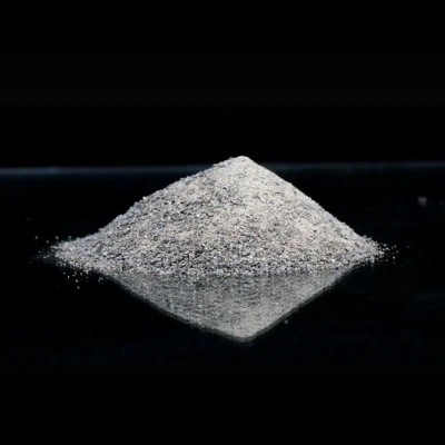
Silicon carbide (SiC) is smelted at high temperature in a resistance furnace using quartz sand, petroleum coke (or coal coke), and wood chips as raw materials. Silicon carbide also exists in nature as a rare mineral, moissanite. Silicon carbide is also called moissanite. Among contemporary non-oxide high-tech refractory raw materials such as C, N, and B, silicon carbide is the most widely used and economical one. It can be called emery sand or refractory sand.

1. The past and present life of silicon carbide
Due to its stable chemical properties, high thermal conductivity, small thermal expansion coefficient, and good wear resistance, silicon carbide has many other uses besides being used as an abrasive, such as coating silicon carbide powder with a special process On the inner wall of the turbine impeller or cylinder block, it can improve its wear resistance and extend its service life by 1 to 2 times; the advanced refractory material made of it is thermal shock resistant, small in size, light in weight, high in strength, and has good energy saving effect. Low-grade silicon carbide (containing about 85% SiC) is an excellent deoxidizer. It can speed up steelmaking, facilitate control of chemical composition, and improve the quality of steel. In addition, silicon carbide is also widely used in the production of silicon carbide rods for electric heating elements.
Silicon carbide is very hard, with a Mohs hardness of 9.5, second only to the world's hardest diamond (level 10). It has excellent thermal conductivity, is a semiconductor, and can resist oxidation at high temperatures.
Silicon carbide history table
| 1905 | Silicon carbide discovered in meteorite for first time |
| 1907 | The first silicon carbide crystal light-emitting diode is born |
| 1955 | A major breakthrough in theory and technology, LELY proposed the concept of growing high-quality carbonization, and since then SiC has been regarded as an important electronic material. |
| 1958 | The first World Silicon Carbide Conference was held in Boston for academic exchanges |
| 1978 | In the 1960s and 1970s, silicon carbide was mainly researched by the former Soviet Union. By 1978, the grain purification and growth method of "LELY improved technology" was first adopted. |
| 1987~present | A silicon carbide production line was established based on CREE's research results, and suppliers began to provide commercialized silicon carbide bases. |
2. Advantageous characteristics of silicon carbide devices
Silicon carbide (SiC) is currently the most mature wide-bandgap semiconductor material. Countries around the world attach great importance to the research of SiC and have invested a lot of manpower and material resources in active development. The United States, Europe, Japan, etc. are not only Corresponding research plans have been formulated at the national level, and some international electronics giants have also invested heavily in the development of silicon carbide semiconductor devices.
Compared with ordinary silicon, components using silicon carbide have the following characteristics:
High-voltage characteristics:
Silicon carbide devices are 10 times the voltage resistance of equivalent silicon devices.
The voltage resistance of silicon carbide Schottky tubes can reach 2400V.
Silicon carbide field effect tubes can withstand voltages of tens of thousands of volts, and their on-state resistance is not very large.

High frequency characteristics:

High-temperature characteristics:
Today, when Si materials are close to the theoretical performance limit, SiC power devices have always been regarded as "ideal devices" and are highly anticipated because of their high withstand voltage, low loss, high efficiency and other characteristics. However, compared with previous Si material devices, the balance between performance and cost of SiC power devices and their demand for high technology will become the key to whether SiC power devices can truly become popular.

At present, low-power silicon carbide devices have entered the practical device production stage from the laboratory. At present, the price of silicon carbide wafers is still relatively high, and they also have many defects. Through continuous research and development, it is expected that silicon carbide devices will dominate the power device market by around 2010. But this is not the case.
3. What is the current development situation of silicon carbide devices?
1. Technical parameters: For example, the Schottky diode voltage increases from 250 volts to more than 1,000 volts, the chip area is smaller, but the current is only a few tens of amps. The operating temperature is increased to 180°C, which is far from the introduction of 600°C. The voltage drop is even more unsatisfactory, it is no different from silicon material, and the high forward voltage drop must reach 2V.
2. Market price: about 5 to 6 times that of silicon material manufacturing.
4. What are the difficulties in the development of silicon carbide ( SiC ) devices? The problem in the development of silicon carbide devices is not the principle design of the chip, especially the chip structure design. It is not difficult to solve it. The difficulty lies in realizing the manufacturing process of the chip structure. Examples are as follows: 1. Micropipe defect density of silicon carbide wafers. 2. The epitaxial process efficiency is low. 3. The doping process has special requirements.
4. Production of ohmic contact. 5. Temperature resistance of supporting materials.
The above are just a few examples, not all. There are still many process problems that have no ideal solutions, such as the silicon carbide semiconductor surface trenching process, terminal passivation process, and the impact of the interface state of the gate oxide layer on the long-term stability of silicon carbide MOSFET devices. Has the industry yet reached a consensus? Consistent conclusions, etc., have greatly hindered the rapid development of silicon carbide power devices.
5. Development overview of main application fields of silicon carbide
Currently, the third generation of semiconductor materials is causing a revolution in clean energy and a new generation of electronic information technology. Whether it is lighting, household appliances, consumer electronics equipment, new energy vehicles, smart grids, or military supplies, these high-performance semiconductors are Materials are in great demand. According to the development of third-generation semiconductors, its main applications are semiconductor lighting, power electronic devices, lasers and detectors, and four other fields.
1. Semiconductor lighting
Among the four application fields, the semiconductor lighting industry has developed the fastest and has formed an industry scale of tens of billions of dollars.
2. Power electronic devices
In the field of power electronics, the application of wide bandgap semiconductors has just started, and the market size is only a few hundred million US dollars. Its application is mainly concentrated in the field of military cutting-edge equipment and is gradually expanding to the civilian field.
3. Lasers and detectors
In the field of laser and detector applications, GaN-based lasers can cover a wide spectrum range and realize the manufacturing of blue, green, and ultraviolet lasers and ultraviolet detection.
4. Other applications
In the field of cutting-edge research, wide bandgap semiconductors can be used in solar cells, biosensors, water-based hydrogen production media, and other emerging applications. Currently, these hot areas are still in the laboratory research and development stage.
Previous: Aluminum Oxide Microgrits